
In semiconductor manufacturing, many of the most yield‑limiting defects are not obvious pattern failures. They are subtle surface anomalies, hidden in plain sight.
Darkfield scatter inspection is designed to expose these issues by making the invisible visible.
By suppressing reflected light and collecting only scattered light, it delivers high-contrast imaging of particles, micro‑scratches, contamination, and sub‑micron defects that would otherwise go unnoticed. This makes darkfield one of the most widely deployed and trusted defect detection techniques in modern semiconductor fabs looking to scale to high-volume manufacturing.
How does Darkfield Scatter Inspection work?
At its core, darkfield scatter inspection operates on a simple principle: perfect surfaces do not scatter light.
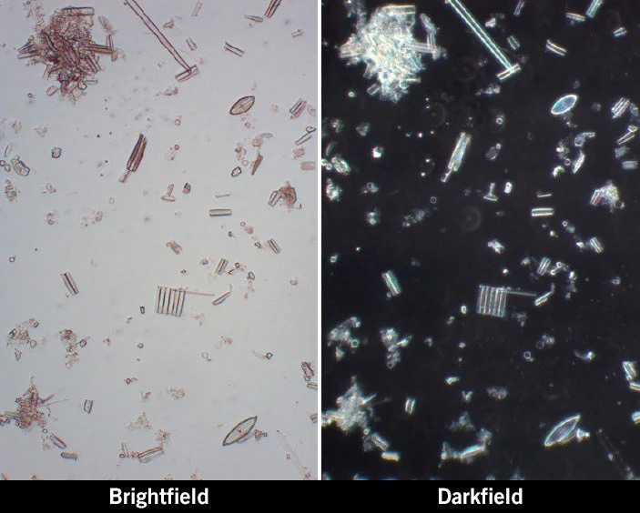
Darkfield detects defects by capturing light scattered from surface irregularities against a dark background, rather than reflecting light from smooth or patterned features.
Smooth films and well‑formed, patterned structures reflect light away from the detector.
As a result, they contribute little to the final image and appear dark. Any defects or irregularities redirect scattered light toward the detector and appear bright.
This approach fundamentally differs from brightfield inspection, which relies on reflected light to assess pattern fidelity. Darkfield does not attempt to measure what the wafer looks like when everything is correct – it isolates and amplifies what is different, abnormal, or unexpected.
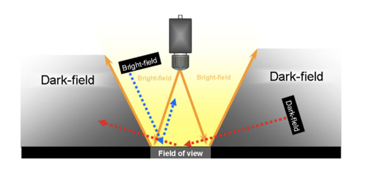
Darkfield inspection systems are carefully engineered to isolate scattered light while minimizing background signal. Several optical design elements work together to achieve this:
- Specular reflection is blocked, preventing smooth surfaces from contributing background signal.
- Oblique illumination uses a slanting, low-angle light to only allow scattered light to enter the imaging lens.
- Scattered light from the edges, particles, and roughness is collected at controlled angles using high-aperture optics.
Semiconductor devices are shrinking; and brightfield inspection is limited when it comes to detecting defects in miniature, complex structures.
This makes darkfield illumination essential to semiconductor inspection. It is one of the primary defect detection techniques used in semiconductor fabs, where surface integrity is a vital factor.
Think of darkfield inspection as a flashlight illuminating the floor of a garage.
The floor itself may look uniform, but every time the beam hits dust, debris, or a surface imperfection, it refracts and produces a bright spot.
Under bright overhead lights, you might notice a spill on the floor, but with angled illumination, the edges of that spill stand out immediately.
Darkfield inspection works the same way.
Smooth surfaces remain dark, while anything that disrupts uniformity scatters light and becomes visible.
Why Darkfield Illumination Is Challenging in Semiconductor Inspection
While the principle behind darkfield scatter inspection is simple, implementing it in semiconductor tools is not. Darkfield illumination inspection applications face a unique mix of space, heat, and optical constraints.
One of the biggest challenges is the limited space above the wafer.
This space must accommodate optics, mechanical components, and chemical exposure considerations, often leaving only a very thin illumination field—on the order of about ¼ inch. Within that constraint, there is little room to introduce high‑power light sources, manage heat, and shape the beam effectively.
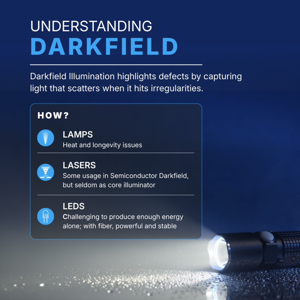
Heat management is especially critical.
While LEDs are slowly becoming more adopted, delivering sufficient optical power for darkfield inspection can require hundreds of watts of electrical input. The power level density is comparable to placing a heat lamp directly above a sensitive wafer, which brings risk to a tightly controlled semiconductor environment.
This is why fiber‑based illumination has traditionally played a key role in darkfield systems. Often described as “cold light sources,” fiber optics allows only the usable light to reach the material while keeping heat‑generating components physically separated from the inspection zone.
Because darkfield performance depends on minimizing stray light and maximizing useful scatter, illumination systems must deliver light precisely while balancing these limitations.
TechniQuip’s TALON illumination platform, solves these problems by combining solid-state LED sources with fiber-based delivery and beam shaping. Rather than flooding the component with light, TALON is designed to deliver only the light that contributes to useful scatter, helping maximize signal‑to‑noise ratio while managing heat and space constraints.
See how TALON can be integrated into your semiconductor workflow today.
Key Use Cases for Darkfield Scatter Inspection
Darkfield scatter is optimized for defects defined by surface disruption, making it indispensable across multipole stages of semiconductor manufacturing.
Particle & Contamination Detection
The most common application of darkfield inspection is particle detection. Even the smallest particle can contaminate the component and negatively impact surface integrity and high-yield production.
Darkfield is routinely used to detect:
- Nanoparticles that the human eye can’t see
- Residue and post‑CMP contamination
- Lithography debris
- Scratch fragments
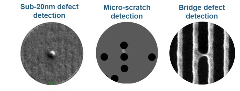
Detecting these requires enhanced detection sensitivity, often seen in systems with higher power, shorter UV wavelengths, and optimized light utilization. Modern systems can reach tens of nanometers, making darkfield suitable for advanced semiconductor processes.
Micro‑Scratches and Surface Irregularities
Not all defects are discrete particles. Small scratches, stringers, and subtle surface irregularities can compromise an imaging system.
Darkfield inspection is highly sensitive to:
- Micro‑scratches
- Thin stringer defects
- Small protrusions
- Surface pits
- Surface roughness variations
These defects produce little contrast and reflected light in brightfield inspection but scatter light efficiently under darkfield illumination, making them easier to identify and track.
Patterned Wafer Defect Detection
On patterned wafers, darkfield scatter inspection can be paired with brightfield methods to reveal defects associated with pattern integrity rather than dimensional accuracy. Often used in lithography or etching steps, darkfield inspection produces a higher defect-to-pattern contrast for dense materials.
Commonly detected issues include:
- Micro‑bridges
- Line breaks or missing patterns
- Pattern edge defects
- Line edge roughness (LER) variations
By amplifying scattered light rather than the reflected signal, darkfield inspection makes these pattern‑related defects easier to detect, even in complex layouts. This combination allows fabs to screen for a broader range of defect types without sacrificing throughput.
Early Yield Learnings
Darkfield scatter inspection plays a critical role during early yield learning, when processes are still being tuned, and defect mechanisms are not yet fully understood. At this stage, the goal is not only to find known defect types, but to surface unexpected anomalies that may indicate emerging process risks.
Because darkfield is highly sensitive to even minor surface disruptions, it is particularly effective at revealing small, isolated defects that may not immediately correlate to known failure modes. These signals can point to early process excursions, material interactions, or tool‑induced variability that would otherwise go undetected.
In R&D and production environments, this sensitivity enables engineers to identify “unknown unknowns” early in development, compare process splits and experimental conditions, and detect subtle changes in surface quality before yield impact becomes visible — ultimately, saving costs and throughput.
AI and Advanced Packaging
There is a big shift in the semiconductor industry towards advanced packaging. Applications to characterize surface integrity and cleanliness are as critical as pattern fidelity. That’s where darkfield scatter inspection adds tremendous value.
Because many advanced packaging structures involve complex topography and multiple material interfaces, traditional reflection‑based inspection can struggle to maintain contrast. Darkfield, by contrast, highlights surface irregularities regardless of pattern complexity, making it well‑suited for screening packaging layers where subtle defects can compromise mechanical or electrical reliability.
Darkfield Scatter Inspection is Now Essential to Quality
As device architectures grow more complex and defect tolerances continue to shrink, visibility becomes everything. Darkfield scatter inspection delivers that visibility by transforming subtle surface disturbances into clear, actionable signals.
Within inspection processes, darkfield is often used as a fast, inline screening step; it flags suspect areas before wafers or other components move through the quality and inspection workflow. This helps manufacturers maintain throughput while protecting yield, even as packaging flows and device structures become increasingly complex.
By prioritizing contrast over reflection, darkfield enables earlier defect detection, faster learning cycles, and more robust process control, cementing its role as a foundational technique in modern semiconductor inspection.
Turning Insights into Action with TechniQuip
As darkfield scatter inspection becomes necessary for modern semiconductor manufacturing, illumination plays an increasingly critical role in inspection performance. TechniQuip’s TALON™ illumination platform is designed to support high‑contrast darkfield applications by delivering controlled, stable light where it matters most.
Learn how TALON can support your darkfield inspection requirements.